Silicon Wafer Resizing/Coring Services
MPE, Inc. offers incredibly accurate and efficient silicon (Si) and silicon on insulator (SOI) wafer resizing. Our resizing process can also be applied to other wafer materials such as glass or germanium. Wafer resizing is sometimes referred to as wafer coring, re-sizing, cut down, cut-down, downsizing, down-sizing, size reducing or size reduction. We can accept orders ranging from a single wafer to hundreds of wafers per month. Our process is efficient, innovative, and ESD friendly. Our proprietary process causes less stress to the silicon wafer than other resizing methods. We also round wafer edges to eliminate edge chipping. We frequently work with 2” (50 mm), 3” (75 mm), 100 mm (4”), 125 mm (5”), 150 mm (6”), 200 mm (8”), and 300 mm wafers; however, we are also capable of producing custom non-standard sizes.
Capabilities
The following are our wafer resizing capabilities:
- Process any wafer diameter up to 300mm
- Process wafers as thin as 0.150mm
- Achieve completed resized wafers anywhere from 50mm to 200mm
- Produce multiple resized wafers from a single wafer. For example, we can produce two 100mm wafers from a single 200mm wafer.
- Produce SEMI-standard flat +/- 0.02 degrees
- Produce SEMI-standard notch in resized wafers
- Spin-coat a protective layer of photoresist prior to resizing
- Tolerance of +/- 0.100mm on the OD dimension
- Offset the wafer center to maximize the die yield
- Laser scribe the wafer ID on the resized wafer for wafer identity control
- Wafer edge rounding / beveling
- High-purity deionized (DI) water grinding coolant
- Trim, thin, or step the edge of resized wafers
- Dice complete die from remnants of original wafer
- We work with fan out wafers, which are also known as reconstructed wafers, WLP (wafer level packaging), WL-CSP (wafer level chip scale package), and reconstituted wafers.
- We work to have your project turned around as quickly as possible and can process your order with a one day turnaround, if necessary
We have the following ESD preventions in place:
- Wrist Straps
- Anti-static mats
- Ion generators
- ESD dicing film
- ESD smocks and gloves
- Ionized air guns
- ESD training and verification protocols
For any additional questions about our wafer resizing services, please call us at 1-877-MPE-DICE, contact us via email, or fill out the request a quote form.
Wafer Resizing: Rounded Edge Profiles
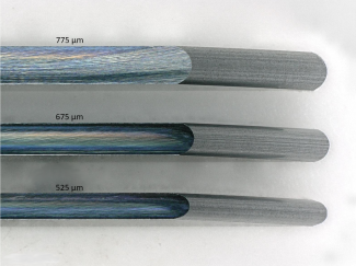
Pictured above are Si wafer cross sections with rounded edge profiles created by MPE's wafer resizing process. MPE can control edge shape to suit a variety of wafer thicknesses.
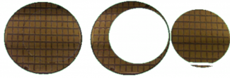
Wafer Resizing: Notch Creation
Shown above is an example of a notch created by MPE in a 200mm Si wafer. MPE can create new notches in resized wafers while maintaining accuracy of orientation relative to crystal plane or patterning. MPE's notch dimensions and tolerances satisfy industry requirements for Si wafers published in SEMI M1.
Many customers utilize MPE to resize both patterned device wafers (i.e. silicon CMOS) and bare or coated (blanket film) wafers to a variety of SEMI-standard wafer diameters. Read example wafer resizing customer scenarios.